Within the EP R&D the module work package (WP 1.3) focusses on the study and development of new module concepts for hybrid and CMOS pixel detectors and their integration for future applications continuing and building on existing activities in the department. It comprises study of enabling technologies, such as interconnection technologies, post processing and packaging, as well as integration concepts for standard and ultrathin silicon pixel detectors and the implementation into an overall detector system, including cooling and powering. Test and qualification of components and assembly and test of demonstrator modules are central activities of this work package.
Mailing List (obsolete) WP1.3 CERNBox Area (restricted) WP1.3 Indico Area (restricted)
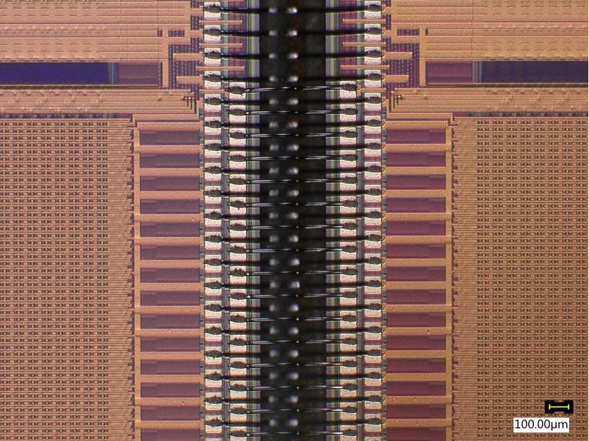
Data and power connection between two MALTA CMOS pixel chips using ultrasonic Al wedge wire bonding
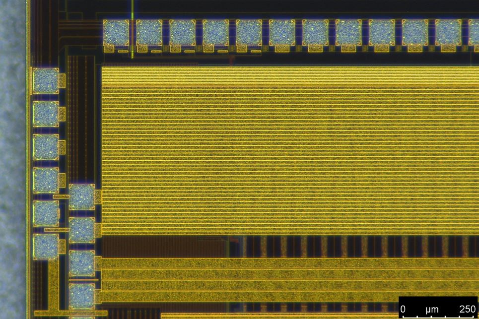
Dicing of MALTA CMOS pixel sensor with minimal dead space at the chip edge.

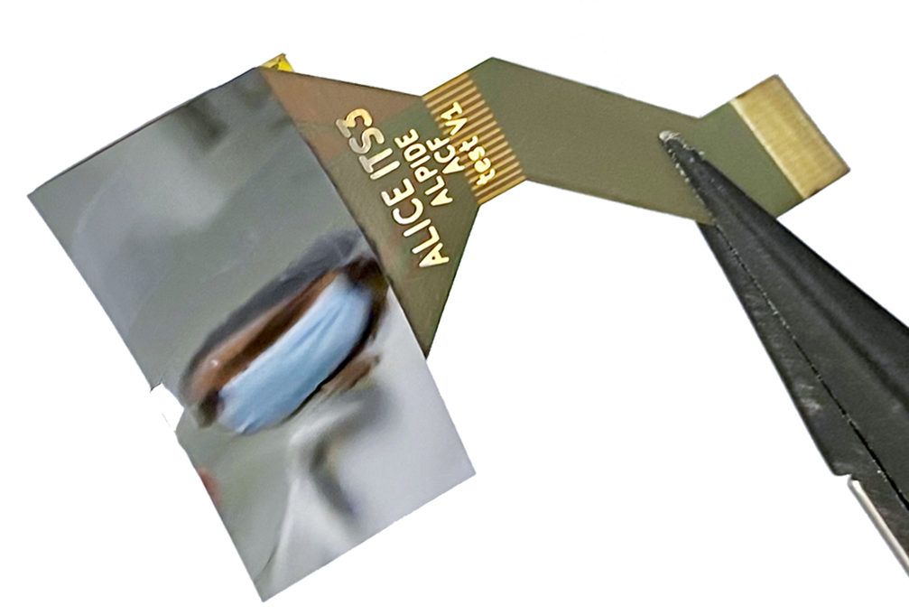
50 micron thick ALPIDE monolithic sensor (15 mm x 30 mm) connected via Anisotropic Conductive Film (ACF) to a flat Kapton cable.

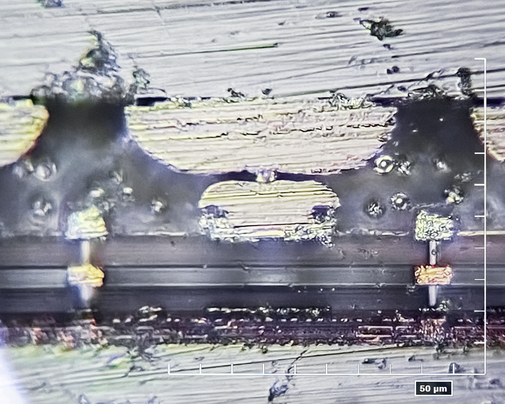
Cross section through a Timepix3 hybrid pixel-detector assembly made with Anisotropic Conductive Film (ACF). Electrical contact is established through embedded conductive micro-particles located between pads of the sensor on top and of the Timepix3 readout ASIC on the bottom.

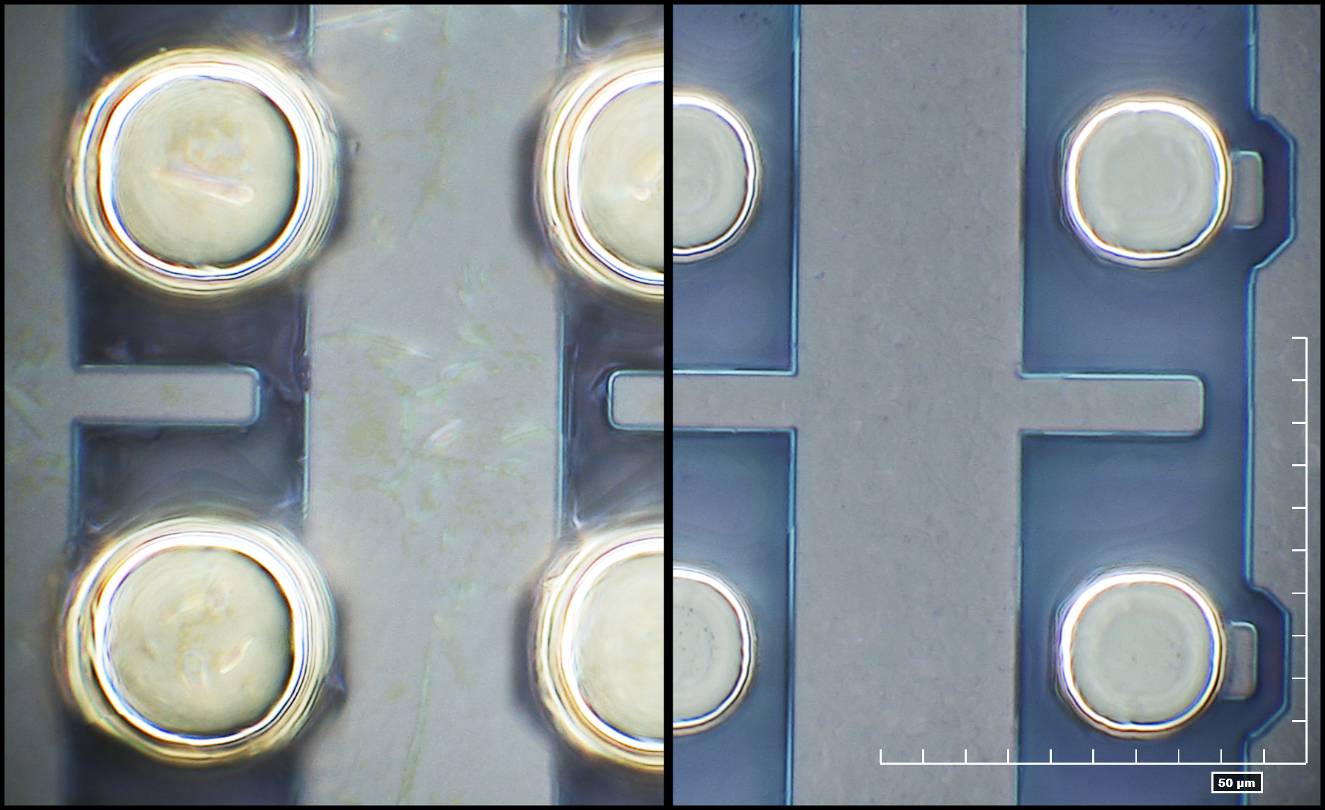
Electroless Nickel Immersion Gold (ENIG) plating on the pixel pads of a Timepix3 readout ASIC. Smaller platings from an industrial process (visible on the right side) have been re-worked in the CERN EP-DT-EF chemistry lab, resulting in larger platings (visible on the left side).

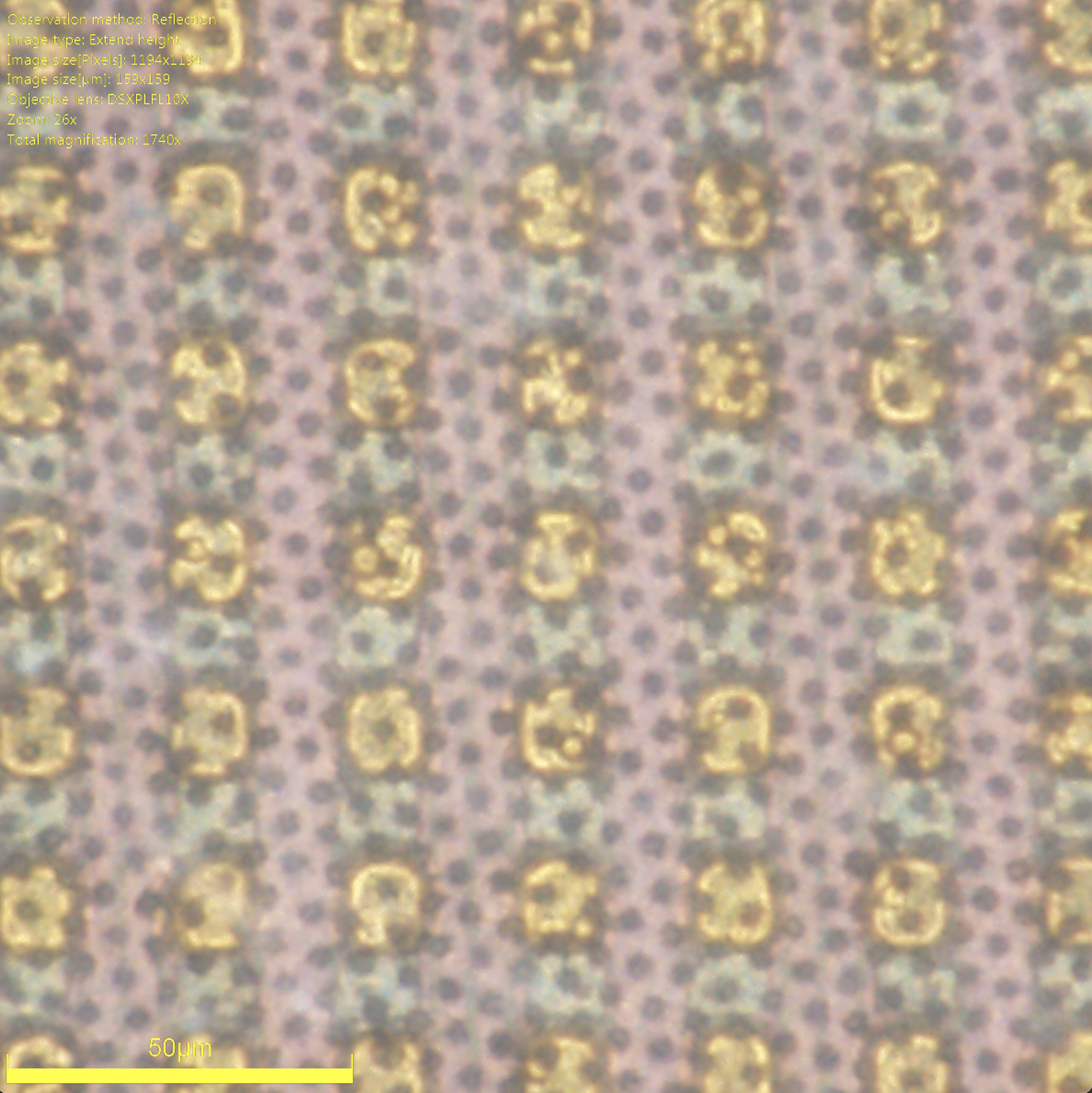
Anisotropic Conductive Film (ACF) with aligned particles on CLICpix2 hybrid readout ASIC.

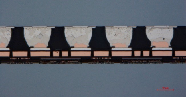
Fine-pitch hybrid pixel assembly with SnAg solder bumps connecting a CLICpix2 chip at the bottom to a planar silicon sensor on top (picture courtesy of IZM).

